Overview
Introduction
In this lab, you will explore transistor circuits. A very brief theory is given below. Much more detail can be found in this Wikipedia article. You will build circuits to observe the transistor as a switch and as an amplifier.
Theory of Bipolar Junction Transistors
The transistor is two pn-junctions. They can be npn or pnp. Arguably, the more common is the npn because of higher charge mobility, faster switching, and higher versatility. Because the transistor has three semiconductor regions, there are three electrical connections. A model of a typical transistor package, the TO-92, is shown in Figure 1.
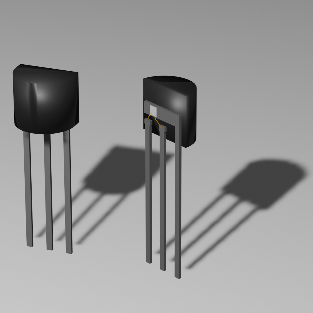
Figure 1:3D model of a TO-92 package, commonly used for small bipolar transistors. The pins from left to right when facing the flat side are specified by the manufacturer. [1]
Circuits with transistors use the circuit diagram symbols shown in Figure 2. We will focus on the npn transistor, but the information presented for npn is similar for pnp transistors, which can to some extent be consider “opposite” to npn transistors. Transistors are considered directional as seen by the diode symbol in Figure 2 that connects the base to the emitter.

Figure 2:The circuit diagram symbol of pnp and npn type bipolar junction transistor (bjt). [2]
A bipolar junction transistor (bjt) is made up of three layers of semiconductor material, each with different electrical properties. These layers are called the emitter, base, and collector. In a pnp transistor, the order is p-type, n-type, then p-type. In an npn transistor, it’s n-type, p-type, then n-type. Each layer is connected to a terminal with the same name: emitter (E), base (B), and collector (C).
The base is a very thin and lightly doped layer placed between the emitter and collector. The emitter sends charge carriers (like electrons or holes) into the base, and most of those carriers get collected by the collector. Because of how the transistor is designed—especially the fact that the collector surrounds the emitter—very few of the charge carriers escape. This makes the transistor very efficient at amplifying current, giving it a high current gain. Transistor current gain, often represented by beta () or , is the ratio of the collector current () to the base current () in a bipolar junction transistor. A cross-sectional of an npn bjt is shown in Figure 3.

Figure 3:A cross-section of the npn type bipolar junction transistor (bjt) collector-emitter-base structure. [3]
One important thing to know about BJTs is that they are not symmetrical. This means you can’t just flip the emitter and collector and expect it to work the same way. If you try to swap them, the transistor goes into what’s called reverse mode, where it works much less effectively. This is because the emitter is heavily doped to push a lot of carriers into the base, while the collector is lightly doped to handle high voltages. The collector–base junction is normally reverse biased (it blocks current), and the emitter–base junction is forward biased (it allows current flow). The way the transistor is built makes sure that most of the current comes from the emitter, which is important for good performance. Performance is determined by a gain parameter, , and a figure of merit, .
Beta () is a useful number that helps describe how well a bipolar junction transistor (bjt) can amplify current. However, it’s not a basic physical constant. It’s more like a helpful shortcut for understanding how the transistor behaves. Technically, BJTs are controlled by voltage, not current. The current flowing from the collector is mainly determined by the voltage between the base and the emitter. The current going into the base happens because of how the base–emitter junction is built, and it can be thought of as an unwanted side effect.
In many circuit designs, engineers assume that beta is large enough that the base current doesn’t significantly affect the circuit’s performance. In other cases, especially in switching circuits (where the transistor is just turned fully on or off), the base current is made large enough to ensure the transistor works properly, even if the transistor has a lower-than-expected beta.
Active Mode
In forward-active or active mode, the base–emitter junction is forward biased and the base–collector junction is reverse biased. Most bipolar transistors are designed to provide the greatest common-emitter current gain, , in forward-active mode. If this is the case, the collector–emitter current is approximately proportional to the base current, but many times larger, for small base current variations.
Figure 4 and Figure 5 show a circuit diagram of an npn transistor connected to two power sources. The applied voltage at the base causes the base-emitter pn-junction to become forward biased, allowing a flow of electrons from the emitter into the base (current from base to emitter). The reverse bias between the collector and base, the electric field existing between base and collector (caused by ) will cause the majority of these electrons to cross the upper pn-junction into the collector to form the collector current . The remainder of the electrons recombine with holes, the majority carriers in the base, making a current through the base connection to form the base current, . As shown in Figure 4 and Figure 5, the emitter current, , is the total transistor current, which is the sum of the other terminal currents, (i.e. ).
Figure 4 and Figure 5 indicate the traditional current with the arrows. The flow of electrons would be in the opposite direction of these arrows because electrons carry negative electric charge. In active mode, the ratio of the collector current to the base current is called the DC current gain . This gain is usually 100 or more, but robust circuit designs do not depend on the exact value (for example see Chapter 8). The value of this gain for DC signals is referred to as . When there are small changes in currents, the value of this gain is referred to as . In other words, under a steady state condition
is used interchangably for both and The emitter current is related to exponentially. At room temperature, an increase in by approximately 60 mV increases the emitter current by a factor of 10. Because the base current is approximately proportional to the collector and emitter currents, they vary in the same way.

Figure 4:An npn bjt with forward-biased B–E junction and reverse-biased B–C junction. [4]

Figure 5:npn bjt with forward-biased B–E junction and reverse-biased B–C junction. An alternative view of an npn bjt with forward biased b-e junction and reverse biased b-c junction. npn bjt with forward-biased B–E junction and reverse-biased B–C junction. [5]
Band Theory
BJTs can be thought of as two diodes (pn-junctions) sharing a common region that minority carriers can move through. The npn transistor is as if two diodes were sharing a P-type anode region. Connecting two diodes with wires will not make a bjt, since minority carriers will not be able to get from one pn-junction to the other through the wire.
BJTs function by letting a small current input to the base control an amplified output from the collector. This current occurs from a voltage bias on the base that lowers the energy of the p-type base. The lower the base energy is the more current that can flow from collector to emitter in the active mode. The result is that the bjt makes a good switch that is controlled by its base input turning on or off the current from collector to emitter. The bjt also makes a good amplifier, since it can multiply a weak base input signal to about 100 times its original strength with the addition of the current-emitter current. BJTs can be networked to build powerful amplifiers for many applications. A band diagram of an npn transitor is shown in Figure 6 and Figure 7.

Figure 6:Band diagram of an npn transistor in equilibrium (no bias). [6]

Figure 7:Band diagram for npn transistor in active mode, showing injection of electrons from emitter to base, and their overshoot into the collector. [7]
Experiments
Part 1 - The Transistor Switch
Build the bjt switch circuit shown in Figure 8.

Figure 8:An npn bjt transistor circuit designed to operate as a switch.
The switch is simply a wire that you can insert or remove one end of to make or break the connection between the +5 V source and the 1 k resistor.
Part 2 - Buffering a Load with the Voltage Divider
In Part 4 - Application: Voltage Divider to Measure Temperature, we learned about voltage dividers. Consider a situation where the known resistor is some unwanted resistance that affects the unknown resistance of a load (device we want to operate). If the known resistor were large compared to the unknown load resistor, we would experience a drop in voltage being applied to our load we want to power. This will affect the performance and maybe the lifetime of our load device. Build a voltage divider with and .

Figure 9:(a) A typical voltage divider circuit. (b) A voltage divider circuit with a load in parallel to a comparably-sized resistor.
Now build the “buffer” circuit in Figure 10 with the base connection going to the output of the voltage divider.

Figure 10:An npn bjt transistor circuit designed to buffer a low impedance load.
Note: such a circuit becomes very useful when interfacing with computers as the data boards generally have low output impedances compared to standalone power supplies.
Part 3 - Constant Current Source
This circuit produces a nearly constant current through a load resistor connected to the collector. The collector current is controlled by the base current in this circuit.

Figure 11:An npn bjt transistor circuit designed to provide constant current to a load.
Part 4 - The Transistor Amplifier
Build the following transistor amplifier; don’t worry too much about the actual design of the circuit – just note that with an ideal BJT it has a gain of 100 (in actuality, it will be closer to 50) without the feedback. Use the largest valued capacitors you can find ().

Figure 12:An npn bjt transistor circuit designed to amplify and input (a) with and (b) without feedback.
Image by Bazylevnik0 - Own work, CC BY-SA 4.0, https://
commons .wikimedia .org /w /index .php ?curid = 130428568 Image by Osbert Joel for Electrical Classroom - Own work, CC BY-SA 4.0, https://
commons .wikimedia .org /w /index .php ?curid = 106111550 Image by Inductiveload - Own work, Public Domain, https://
commons .wikimedia .org /w /index .php ?curid = 11068760 Image by Jp314159 - Own work, CC BY-SA 4.0, https://
commons .wikimedia .org /w /index .php ?curid = 78389923 Image by Inductiveload - Own workBased on File:Npn-structure.png, by User:Heron at the English Wikipedia, CC BY-SA 3.0, https://
commons .wikimedia .org /w /index .php ?curid = 11068618 Image by Inductiveload - Own drawing, done in Inkscape, Public Domain, https://
commons .wikimedia .org /w /index .php ?curid = 1696512 Image by Inductiveload - Own drawing, done in Inkscape, Public Domain, https://
commons .wikimedia .org /w /index .php ?curid = 1696520